
Exclusive Design Feature
ISSUE: September 2009
|
Switching-Regulator Insights: Achieve Longer Battery Life in DSP Systems Attaining high performance and low power consumption in MP3 players, personal media players, digital cameras, and other portable consumer applications has long been a challenge for designers. These battery-powered systems typically employ an embedded digital signal processor (DSP) to achieve maximum processing power when handling multimedia applications and minimum power consumption when in sleep mode. Naturally, battery life is of prime importance in handheld battery-powered products, making their success directly related to the efficiency of the power system. A key component of such systems is the stepdown dc-dc switching regulator, which is also commonly referred to as a stepdown dc-dc converter or buck converter. A stepdown switching regulator efficiently derives a low supply voltage, say 1 V, from a higher-voltage supply such as 4.5 V. As a regulator, it must maintain a constant voltage, rapidly responding to variations in the upstream supply or the load current. There are numerous stepdown switching regulators on the market today for use in DSP-based battery-powered products. These regulators employ various control schemes to achieve their static and dynamic performance, and they offer various levels of functional capability. Here, we’ll look at a new stepdown switching regulator architecture that provides good regulation, high efficiency, and fast response in DSP-based, battery-powered applications. The regulator employs a constant on-time, valley-current-mode control scheme, known as leading-edge modulation, which is described along with other details of regulator circuit operation. Waveforms are presented to show the regulator’s performance in a typical application. (An appendix to the article compares constant on-time, valley-current-mode control with the conventional constant-frequency peak-current control scheme.) With that information as background, the requirements for dynamic voltage adjustment in DSP-based systems and the benefits of using an external regulator for dynamic voltage adjustment are discussed. Finally, two methods are presented for adjusting the DSP’s core voltage using a synchronous dc-dc converter to dynamically adjust the core voltage to values from 1.2 V to 1.0 V when the processor is running at a reduced clock speed. The regulator featured in these discussions, the ADP2102, employs the new regulator architecture described earlier in the article.
Anatomy
Of A Switching Regulator
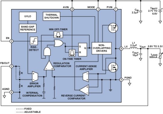
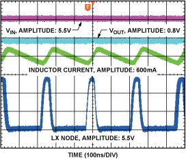
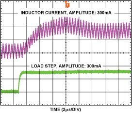
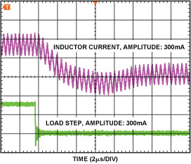
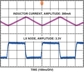
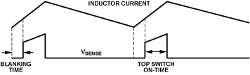
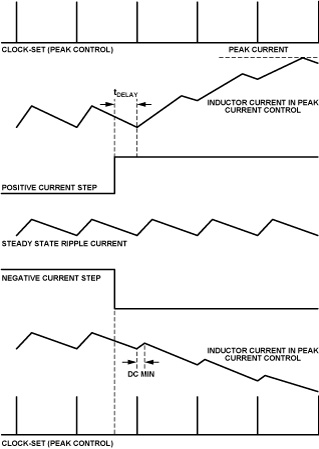
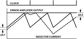
The stepdown converter circuit operates as follows: A fraction of the dc output voltage is compared with an internal reference in the error amplifier. The output of the error amplifier is then compared with the output of a current-sense amplifier to drive a one-shot that is on for a period of time that depends on the ratio VOUT/VIN. The one-shot turns on the upper gating transistor and the current in inductor L1 ramps up. When the one-shot times out, the transistor is turned off, and the current ramps down. After an interval determined by the minimum-off-timer and the minimum (“valley”) current, the one-shot is pulsed again. The on-chip one-shot timer employs input-voltage feedforward for maintaining a constant frequency in the steady state. This switching continues indefinitely—at approximately 3 MHz, but deviating as necessary to respond to transient line and load changes—maintaining the output voltage at the programmed value and the average inductor current at the value required by the output load. The approach described above, which is relatively new, is called constant on-time, valley-current-mode control. It’s also known as leading-edge modulation. This control method differs from the conventional approach to dc-dc conversion: constant-frequency peak-current mode control, which is alternately referred to as trailing-edge modulation. That approach has been used for many years in stepdown dc-dc converters. (For a description of constant-frequency peak-current-mode control, and an evaluation of its strengths and weaknesses vis-à-vis the constant on-time valley-current-mode control, see the appendix “Advantages of Constant On-Time Valley-Current-Mode Control Scheme In Stepdown DC-DC Converters” following this article.) A stepdown converter such as the ADP2102 also includes undervoltage lockout, soft start, thermal shutdown, short-circuit protection, and ±1% feedback accuracy. This architecture allows the on-time of the main switch to go as low as, or lower than, 60 ns. Figure 2 shows typical waveforms under various conditions. Figure 2a shows the low duty cycle that accompanies the large voltage reduction from VIN = 5.5 V to VOUT = 0.8 V at ILOAD = 600 mA. As can be seen in the plot, the minimum on-time achieved is 45 ns with a switching frequency of 3 MHz. Figure 2b shows the load current and inductor current in response to a 300-mA step increase in load current. Figure 2c shows the load current and inductor current in response to a 300-mA step decrease in load current. Figure 2d shows that there are no subharmonic oscillations when the part operates at a 50% duty cycle, which is a concern for parts using peak-current-mode control. This freedom from subharmonic oscillations is also the case for duty-cycle values somewhat greater or less than 50%.
Dynamic
Voltage Adjustment In A DSP Application Described here are improvements in system power efficiency that can be attained in battery-powered applications by replacing the internal regulator of a DSP such as Analog Devices’ Blackfin with an external high-efficiency regulator. Also described is the control software for the external regulator.
Dynamic
Power Management Changing the clock frequency—but not the supply voltage—in a power-sensitive application is useful when the DSP is simply monitoring activity or waiting for an external trigger. In high-performance battery-powered applications, however, merely changing the frequency may not save enough power. Processors such as the Blackfin, and other DSPs with advanced power-management features, allow the core voltage to be changed in tandem with frequency changes, thus seeking optimal loading of the battery for each situation. Dynamic voltage regulation in processors is typically implemented with an internal voltage controller and an external MOSFET. The advantage of this approach is that a single voltage (VDDEXT) can be applied to the DSP subsystem, while the DSP derives the necessary core voltage (VDDINT) from the MOSFET. Internal registers allow the regulated core voltage to be software-controlled in order that the MIPS, and ultimately the consumed energy, can be coordinated to achieve optimal battery life. To fully implement this internal processor’s regulator scheme requires an external MOSFET, a Schottky diode, a large inductor, and multiple output capacitors—a relatively expensive solution with poor efficiency that uses a relatively large PCB area. The use of the large inductors and capacitors required by the integrated regulator brings the system designer into conflict with consumer desires for portable devices to be as small as possible. Along with the relatively low efficiency of the integrated regulator controller—typically 50% to 75%—this approach is less than optimally suited for high-performance, handheld, battery-powered applications.
External
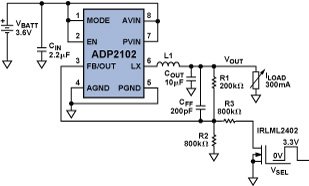
Regulation A variety of dynamic voltage-scaling (DVS) control schemes are available, ranging from switched resistors—which in some cases can be implemented by using a DAC—to pulse-width modulation (PWM), which can achieve as fine a granularity as the internal method. Whatever scheme is used must provide the ability to change the regulation level via software control. While this regulation control method is inherent with the internal regulator approach, it must be added in external approaches. This article describes two ways to adjust the DSP’s core voltage using a synchronous buck converter, such as the ADP2102 to dynamically adjust the core voltage to values from 1.2 V to 1.0 V when the processor is running at a reduced clock speed. Figure 3 illustrates a circuit that implements DVS. The 3.3-V system power supply on the processor’s board powers the buck converter, whose output voltage is set to 1.2 V using the external resistive divider comprised of R1 and R2. A GPIO pin from the DSP is used to select a requested core voltage. Varying the feedback resistor adjusts the core voltage from 1.2 V to 1.0 V. An N-channel MOSFET (the IRLML2402) modifies the voltage divider by inserting resistor R3 in parallel with R2. The 0.25-ohm RDS(ON) of the IRLML2402 is small compared to R3. The 3.3 V GPIO voltage is used to drive the MOSFET gate. Feedforward capacitor CFF is needed for better transient performance and improved load regulation.
Figure 3. Dynamic voltage scaling of ADP2102 using an external MOSFET and Blackfin PWM control. The general application requirements for two-level switching are:
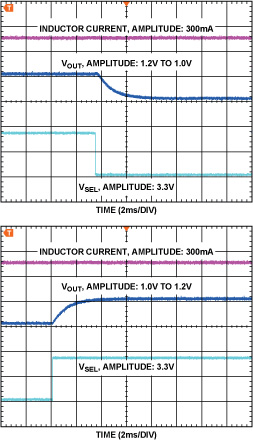
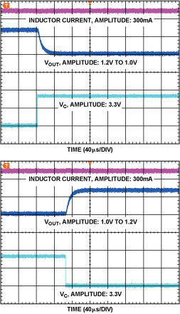
High-value resistors are used to minimize power losses through the resistive divider. The feedforward capacitor reduces the effect of the gate-to-drain capacitance during switching. The overshoot and undershoot caused during this transition can be minimized by using smaller feedback resistors and a larger feedforward capacitor, but only at the expense of additional power dissipation. Figure 4 shows the output current, IOUT, output voltage, VOUT, and control voltage, VSEL. A low level on VSEL scales the output voltage to 1.0 V, and a high level on VSEL scales it to 1.2 V.
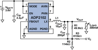
Figure 4.Modulating the bottom feedback resistor with a MOSFET. A simpler way to generate two different voltages for DVS uses a control voltage, VC, to inject current into the feedback network through an additional resistor. Adjusting the duty cycle of the control voltage varies its average dc level. A single control voltage and resistor can thus be used to adjust the output voltage. The following equations are used to calculate the values of resistors R2, R3, and the control-voltage amplitude levels, VC_LOW and VC_HIGH.
With VOUT1 = 1.2 V, VOUT2 = 1.0 V, VFB = 0.8 V, VC_LOW = 3.3 V, VC_HIGH = 0 V, and R1= 49.9 kohm, R2 and R3 can be calculated as follows
This approach produces much smoother transitions. Any control voltage that can drive resistive loads can be used for this scheme, as opposed to the MOSFET switching approach, which can only be used with control signal sources that can drive capacitive loads. This approach can be scaled to any output voltage combinations and output load currents. Thus, DSP power dissipation can be reduced by scaling the core voltage as needed. Figure 5 shows the implementation of the above scheme. Figure 6 shows the transition between the two output voltages using this current-injection method.
Figure 5.Dynamic voltage scaling of a stepdown converter using control voltage VC.
Figure 6.Modulating the bottom feedback resistor with a control voltage.
For Further Reading:
Tim received a BSEE from Purdue in 1976 and an MSE with Electrical option in 1997 from Southern Illinois University.
Previously, Oliver worked on data converters.
He has 12 years of experience in power-management IC design, applications and marketing. Sridhar has a master’s degree in electrical engineering and is currently working on a master’s degree in business administration.
For further reading on techniques for extending battery life in portable application, see the How2Power Design Guide, and search the Application category and the Battery Powered & Portable Products subcategory. |
 Tim
Wilkerson joined Analog Devices in 2001 as a senior field
applications engineer located in San Jose, Calif. Prior to that Tim
was with STMicroelectronics and Waferscale Integration in central
applications. Previous work includes 20 years in design and
development for several companies in the Midwest, most recently at
Basler Electric working on protective relays for power systems.
Tim
Wilkerson joined Analog Devices in 2001 as a senior field
applications engineer located in San Jose, Calif. Prior to that Tim
was with STMicroelectronics and Waferscale Integration in central
applications. Previous work includes 20 years in design and
development for several companies in the Midwest, most recently at
Basler Electric working on protective relays for power systems.  Oliver
Brennan is a senior IC design engineer with Analog Devices where he has
worked for 12 years. He currently works on Power Management
Products.
Oliver
Brennan is a senior IC design engineer with Analog Devices where he has
worked for 12 years. He currently works on Power Management
Products.  Sridhar
Gurram joined Analog Devices in 2006 and currently is a staff
applications engineer with the company’s Power Management
Products group in San Jose, Calif., focusing on switching regulators
for industrial and infrastructure markets. Earlier, he was a product
marketing engineer for the dc-dc switching regulator product line.
Sridhar
Gurram joined Analog Devices in 2006 and currently is a staff
applications engineer with the company’s Power Management
Products group in San Jose, Calif., focusing on switching regulators
for industrial and infrastructure markets. Earlier, he was a product
marketing engineer for the dc-dc switching regulator product line.