
Exclusive Design Feature
ISSUE: September 2009
|
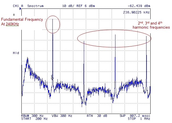
Frequency Dithering: A Tool for Overcoming Last-Minute EMC Hurdles Designing a power converter to meet electromagnetic compatibility (EMC) requirements can be a challenge. A power converter’s high-frequency switching can produce both conducted and radiated electromagnetic interference (EMI) at levels that exceed the acceptable limits. Ideally, designers will minimize the effects of EMI during power-converter circuit design and pc-board layout by applying best engineering practices. There is no substitute for good layout, design and filtering practices, all of which can reduce the power converter’s EMI to acceptable levels and permit the power converter and/or the final product to achieve EMC approvals. However, not every power converter is designed under ideal conditions. Often the emissions of the power converter are not measured until late in the development process when the power converter is integrated into the completed final assembly or system. Usually, at that time there is limited space to add extra filtering components and no time in the schedule to accommodate a redesign. Finding a solution to pass the EMC requirements late in the design cycle can be expensive and time consuming. One relatively simple way to reduce a converter’s peak emissions and possibly pass the EMC requirements is to enable a clock-dithering circuit, which dithers the converter’s switching frequency. This technique is somewhat controversial. Some engineers view it as “cheating the spec” because frequency dithering doesn’t reduce a converter’s overall emissions but rather suppresses peak emissions while raising the overall emissions noise floor. However, others view frequency dithering simply as a smart way to stay on schedule by minimizing late design changes. This article examines some of the issues that arise when frequency dithering is applied to power converter designs and describes two techniques for implementing frequency dithering. Dithering Pros and Cons In a fixed-frequency (clocked) power converter, narrowband emissions typically occur at the fundamental of the switching frequency with successive harmonics having less and less energy. A plot of the conducted emissions for a typical fixed frequency is shown in Figure 1.
Figure 1. Plot of conducted emissions for a typical fixed-frequency converter. Dithering the oscillator frequency results in the power converter being operated not at a single, fixed frequency but over a varying band of frequencies. As a result, the EMI emissions are spread over a range of frequencies instead of a narrow band, resulting in the reduction of the peak value of the EMI emissions. Furthermore, dithering the oscillator will also reduce the peak value at the harmonic frequencies (i.e. frequencies that are multiples of the switching frequency). The extent to which emissions are reduced by dithering depends on the choice of modulating frequency (rate of dithering), the dither bandwidth, modulation wave shape and the receiver’s resolution bandwidth. By proper selection of these parameters, it is possible to lower EMI emissions by 10 dB or more. Frequency dithering will do little or nothing to reduce high-frequency (multi-megahertz) nonharmonic emissions. These emissions are a result of the sharp edges and ringing at the switching node due to parasitic L-C circuits, diode reverse-recovery currents, etc. Adding a snubber, a gate-drive resistor and/or use of a soft-recovery diode are common solutions to reduce these emissions. Furthermore, dithering the oscillator will add a small amount of ripple to the output voltage. The frequency of this output voltage ripple, equal to the dithering frequency, is usually much smaller than the frequency of the output voltage ripple due to capacitor ESR and inductor current (which is same as the switching frequency). When set right, the magnitude of the output ripple due to dithering is relatively low compared to the magnitude of the nominal output ripple. (Later in this article, this issue of output ripple will be discussed within the context of a buck converter design.)
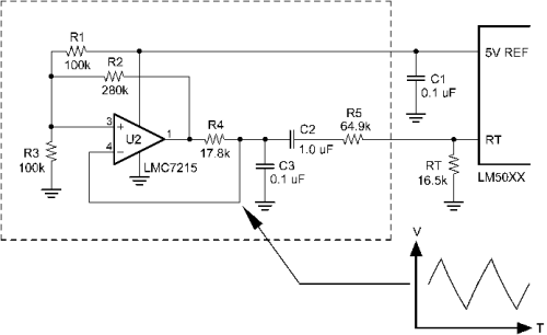
Most modern PWM controllers use an external resistor to set the operating frequency. Typically, the operating frequency increases with decreasing resistor values. Internal to the controller, the oscillator programming pin (RT) is regulated to a constant voltage (2 V in the following example). A programming resistor connected to the programming pin sets the current sourced out of the programming pin. A proportional current is also sourced into an internal timing capacitor. The period of the ramping voltage on the timing capacitor determines the oscillator frequency. The external dithering circuit shown in Figure 2 consists of a simple standalone, comparator-based oscillator. This oscillator is configured to operate at approximately 800 Hz.
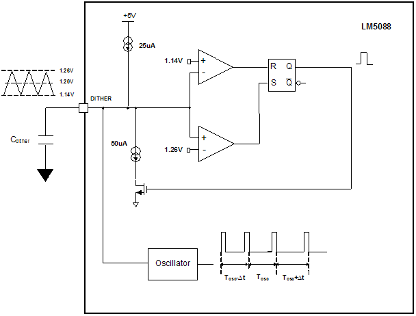
Figure 2. Low-frequency oscillator modulates PWM controller oscillator frequency. Upon power-up, the output state of comparator U2 is high. The initial threshold (set by resistors R1 – R3) of the positive comparator input is 2.9 V. The voltage at the capacitor C3 ramps up to the positive threshold. When the positive threshold is reached, the output of the comparator switches low, which also lowers the threshold at the comparator positive input to 2.1 V. The voltage at capacitor C3 now ramps down towards the new threshold. Once the capacitor voltage reaches the lower threshold the cycle repeats again. The voltage on the C3 capacitor resembles a triangle wave with a minimum valley of 2.1 V and a peak of 2.9 V. The dithering of the PWM oscillator is accomplished by allowing the triangle wave to modulate the current drawn from the controller’s RT pin. Resistor R5 sets the percentage of modulation dither forced upon the PWM oscillator’s base frequency. The right side of R5 is fixed at the regulated RT pin potential of 2.0 V. The low-frequency triangle wave is present on the left side of resistor R5, through coupling capacitor C2. For an R3 value of 64.9 kΩ, the peak-to-peak current through the resistor is 12 µA. The normal current sourced from the RT pin without the dither circuit connected is 121 µA. The 12-µA peak-to-peak dither current represents 10% total modulation. Buck Controller with Dithering Measurements A second implementation of dithering is shown in Figure 3 for a buck converter using the LM5088-1. This IC has a built-in ±5% dithering function.
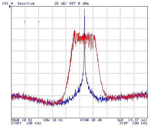
Figure 3: Built-in frequency dithering scheme in LM5088. The dither pin sets the triangle dithering frequency or can be used to disable the dither. As shown in the Figure 3, the Cdither capacitor is used to generate a triangular waveform. This triangular waveform is used to manipulate the oscillator circuit such that the oscillator circuit modulates ±5% of the nominal operating frequency set by the RT resistor. Disabling the dithering is very useful for normal circuit debugging; allowing stable triggering and observation of circuit nodes. Conducted emissions were measured on the evaluation board. The fundamental operating frequency is around 240 kHz, set by the controller’s RT resistor. Shown in the blue trace of Figure 4 are the conducted emissions (on the positive-input power line) for the power converter without the dither circuit applied.
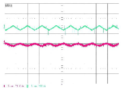
As expected, the peak emissions are narrowly confined around the fundamental oscillator frequency of 240 kHz. When the oscillator dither circuit in Figure 3 is enabled, the conducted emissions are as shown in the red trace of Figure 4. The emissions are now more broadband instead of narrowband i.e. emissions are now spread around the fundamental frequency instead being singularly confined to the fundamental frequency. The measured peak over this frequency band has now been reduced by 20 dB. (Each box on the y-axis is 10 dB). The resolution bandwidth (RBW) for this measurement is set to 200 Hz. The observed effect of dithering may be impacted by the RBW setting. The RBW must be set several times lower than the dithering frequency in order to observe the dithering effect. Many EMC testing standards specify the RBW over specific frequency ranges. So the net observed effect of dithering may be reduced depending upon the RBW setting, fundamental oscillator frequency and modulation frequency. As mentioned earlier, dithering the oscillator circuit will add a slow frequency ripple to the output voltage. Usually the magnitude of this ripple is so small that it cannot be observed through the switching noise. Figure 5 is an ac-coupled output-voltage waveform captured using a low-pass RC filter (R=10 Ω; C= 2 µF) to filter out the switching noise. It was captured by connecting the RC filter in parallel to the output capacitor and by probing the voltage across the 2-µF capacitor. If the dithering rate is lower than the bandwidth of the power converter, then the control loop will try to correct for this additional ripple. In the example shown, the dithering frequency is 1.5 kHz while the bandwidth of the LM5088 evaluation board is 15 kHz. Lowering the dithering frequency further will allow the control loop to correct this additional output ripple.
Planning Ahead Although it was noted previously, this caution bears repeating: When it comes to reducing EMI, there is no substitute for good layout, design and filtering. Frequency dithering can reduce the peak measured emissions at the fundamental clock frequency and lower-order harmonics. However, it does not reduce the overall emitted energy and does little to reduce high-frequency non-harmonic frequency emissions. Nevertheless, if an engineer is faced with the need to reduce the fundamental frequency and harmonic emissions late in the design process, enabling a dithering circuit may save a lot of redesign cost. The dithering circuit can be designed in early and left dormant until the final EMC testing. About the Authors
Prior to joining National, Bob designed power converters for military and space applications. Bob holds a Bachelor of Science degree in Electronic Engineering from Fairleigh Dickinson University. To date he has published 25 power design articles, 8 conference papers and 3 patents.
Prior to National, he worked for General Electric designing power converters for lighting applications. He holds a Master’s in Electrical Engineering from the University of Florida. Ajay has published several papers and articles in the area of power electronics and holds one U.S. patent.
For further reading on how to address EMI and EMC issues, see the How2Power Design Guide, and search the Design Area category and the EMI and EMC subcategory |
 Robert (Bob) Bell is the applications engineering manager for the National Semiconductor design center in Phoenix, Arizona. Products designed at the Phoenix design center include integrated switching regulators, next-generation PWM power controllers, gate drivers, and hotswap and load share controllers. He has been with National Semiconductor since September 2001.
  Ajay Hari is an applications engineer at the National Semiconductor design center in Phoenix, Arizona. He has been with National Semiconductor since 2007.