|
|
IN THIS ISSUE:
» Driver IC Subdues Level-Shifting Losses In Active Clamp Flybacks And Other Applications
» Configurable ICs Build Versatile, Low-Cost Regulated Charge Pumps
» Managing Pulse Top Decay Improves Accuracy Of Current Sensing Circuits
» Focus On Magnetics:
Interbundle Penetration Of Wire Bundles Improves Their Packing Factor
» Spotlight On Safety & Compliance:
Very Down To Earth Treatment Of Grounding For Power Electronics Designers
» New Power Products
» Industry Events:
Symposium Tackled EOS And ESD Challenges Across The Electronics Spectrum Including Power Design
» What's New at HOW2POWER.COM
» In Memoriam: Milan M. Jovanović
» Other Top Power News
From the Editor's Desk David G. Morrison
Editor, HOW2POWER TODAY

Many innovative and powerful concepts in power supply design await the development of new power semiconductors—discretes, modules, and ICs—to propel those concepts into mainstream use. While there are always new semiconductor components promising to make such impact, this issue of the newsletter seems to have more the usual share of examples. First, we have Dhruv Chopra’s article discussing the application of a new high-side low-side gate driver that reduces losses at high switching frequencies. His feature discusses its performance in the active clamp flyback, a topology that’s being targeted for use in adapters. Then, we have Vladimir Veljkovic’s article explaining how to take advantage of configurable mixed-signal ICs to design regulated charge pumps that suit a range of application needs yet may cost less than standalone charge pump ICs. Meanwhile, in the product news section, we have new GaN and SiC devices, a buck-boost chipset, precision current sources, and offline switcher chips that boast new capabilities. Hopefully one of these new components will inspire thoughts of new possibilities in your design work. Or perhaps you’ll find inspiration in other articles such as Gregory Mirsky’s work, which addresses a source of error in current sensing circuits; Dennis Feucht’s magnetics article discussing an issue that arises with wire bundles; or Kevin Parmenter’s review of a book on grounding and bonding. You’ll find these discussions and more in this issue.
|
|
 |
 |
|
HOW2POWER EXCLUSIVE DESIGN ARTICLES 
|
Driver IC Subdues Level-Shifting Losses In Active Clamp Flybacks And Other Applications
by Dhruv Chopra, ON Semiconductor, Phoenix, Ariz.
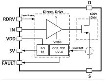
ZVS topologies can eliminate switching losses associated with the power switch. For popular ZVS topologies like LLC half-bridge converters, full-bridge converters, active-clamp flybacks, two-switch forward converters, etc., low−side high−side drivers are needed to perform the function of buffer and level shifter. But there are inherent losses associated with power switch drivers. In topologies like LLC, half- or full bridge converters, which have a totem-pole structure of power switches, level-shifting losses of the high-side driver are significant. These losses become even worse at higher switching frequencies. In response to this need, ON Semiconductor developed the NCP51530, a 700-V high-side low-side driver for ac−dc power supplies and inverters with very low level-shifting losses. This article describes the application of the NCP51530 driver in a 60-W USB Power Delivery (PD) adapter design based on the active-clamp flyback.
Read the full story…
|
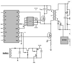
This article compares the performance of the
NCP51530 with two industry-standard drivers
in an active clamp flyback-based adapter design. |
|
The basic design of a GreenPAK
device in a regulated charge pump. |
Configurable ICs Build Versatile, Low-Cost Regulated Charge Pumps
by Vladimir Veljkovic, Dialog Semiconductor, Belgrade, Serbia
Many battery-powered IoT applications require additional voltage levels for powering specific interface circuits, sensors, etc. Under certain operating conditions, charge pumps provide simple, efficient solutions for generating the required supply voltages. While standalone charge pump ICs can be used, charge pumps can also be implemented using a GreenPAK configurable mixed-signal IC (CMIC), which offers several advantages. These include lower cost, smaller size, multiple outputs with the same IC, programmable operating frequency, control via a serial interface, lower quiescent current, and on-chip logic for additional functions. In general, a GreenPAK solution provides the flexibility to shift the design to meet system priorities. This article explains how to design regulated capacitive charge pumps using a GreenPAK CMIC and a few low-cost external components. Read the full story…
|
Managing Pulse Top Decay Improves Accuracy Of Current Sensing Circuits
by Gregory Mirsky, Continental Automotive Systems, Deer Park, Ill.
When a current transformer senses current in switched-mode power supplies and other applications, the current transformer and the associated burden resistor can alter the shape of the switching waveform as seen by the current sensing circuit. This change in the shape of the switching pulse can be described as pulse top decay and it degrades the accuracy of the current sense signal. This article quantifies the effect of the current sensing circuit on the pulse decay, providing guidance on how to properly determine the value of the burden resistor. This article also aims to show that the secondary side of a current transformer should provide the inductance energy discharge through a controllable voltage limiter, which ensures the zero volt-second integral of the current transformer.
Read the full story…
|
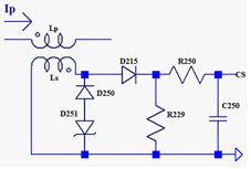
In this current sensing circuit, the time
constant associated with the inductance
of the current transformer’s secondary winding
and the burden resistor can increase the slope
of the pulse top on the output voltage.
|
|  |
FOCUS ON MAGNETICS
Sponsored by Payton Planar Magnetics
A monthly column presenting information on power magnetics design, products, or related technology |
Interbundle Penetration Of Wire Bundles Improves Their Packing Factor
by Dennis Feucht, Innovatia Laboratories, Cayo, Belize
When winding transformers or coupled inductors with twisted wiring bundles, turns of adjacent wire bundles are typically wound close-packed to maximize packing factor (and in particular, porosity packing) and ultimately maximize winding current density. Bundles of a small number of strands can pack together more closely than those with a large number of strands because of the sinusoidal variation in their outside diameter. This article examines the extent to which twisted wire bundles can penetrate each other by fitting into the dips in adjacent windings and thereby increase packing factor. This analysis quantifies the relationship between the number of strands in a twisted wire bundle and the extent to which one wiring bundle penetrates or “meshes with” the other. Read the full story…
|
The shape of a bundle of Ns strands when
viewed from the side of the bundle has a
characteristic ripple along its outer edges. |
|
 |
SPOTLIGHT ON SAFETY & COMPLIANCE
Sponsored by Power Integrations
A monthly column discussing standards and regulatory requirements affecting power electronics |
Very Down To Earth Treatment Of Grounding For Power Electronics Designers
Grounding and Bonding for the Radio Amateur, published by The American Radio Relay League (ARRL), copyright 2017, 176 pages, available in softcover or Kindle edition, ISBN number 978-1-62595-065-9, item number 0659, $22.95 from ARRL.
By Kevin Parmenter, Chair, and James Spangler, Co-chair, PSMA Safety and Compliance Committee
When the subject of ground comes up in power supply design, it’s usually in the context of circuit design or measurement, and the discussion often concerns noise issues in some way. How to layout ground traces and planes to avoid crosstalk, EMI, groundbounce and similar effects. But there’s another side to ground that concerns the safety of equipment, and more importantly, the safety of its operators. This is where the related subjects of grounding and bonding come in, and these are the focus of the book being reviewed here. They’re important because safety, lightning protection, emissions–immunity EMI-EMC and proper system operation overall will depend on how well grounding is done. Read the full story…
|
 |
|
 |
 — POWER PRODUCTS IN 3 IMAGES OR LESS — POWER PRODUCTS IN 3 IMAGES OR LESS
|
|
Texas Instruments’ LMG34x
family of 600-V GaN power stages. |
600-V GaN FET Power Stages Boost Performance For Applications Up To 10 kW
 Diagram: Offered in 8-mm x 8-mm split-pad QFNs, the LMG34x 600-V GaN FET power stages feature an integrated gate driver with zero common-source inductance, a 5-V LDO to power an external digital isolator, an integrated bias supply, and high-speed overcurrent protection. They offer a choice of a 50-mΩ or 70-mΩ GaN FET. Diagram: Offered in 8-mm x 8-mm split-pad QFNs, the LMG34x 600-V GaN FET power stages feature an integrated gate driver with zero common-source inductance, a 5-V LDO to power an external digital isolator, an integrated bias supply, and high-speed overcurrent protection. They offer a choice of a 50-mΩ or 70-mΩ GaN FET.
More details… |
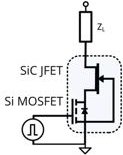
UnitedSiC’s UF3C FAST series
650-V and 1200-V SiC FETs. |
SiC FETs Offer Faster Switching With Cascode Convenience
Chart: The UF3C FAST series is an extension of the company’s SiC FET product line offering faster switching speeds. These are cascode devices combining the company’s SiC JFETs with silicon MOSFETs. The cascode approach simplifies gate drive and allows these devices to serve as “drop-in” replacements for most TO-247-3L IGBTs, silicon MOSFETs and SiC MOSFETs.
See the full story…
|
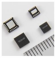
Rohm’s BD8P250MUF-C + BD90302NUF-C buck-boost chipset. |
Automotive Buck-Boost Chipset Meets Demands Of Start-Stop Vehicle Systems
Photo: The buck-boost power supply chipset integrates a buck dc-dc converter with boost functionality and a dedicated boost IC. It is designed for use in automotive ECUs for cluster panels and gateways used in start-stop vehicle systems.
Graphs: When compared with convention buck-boost power supplies, this chipset is said to achieve the industry’s lowest current consumption and fastest response. The chipset maintains a stable output voltage during buck-boost switching with just 44 µF of output capacitance.
See the full story…
|
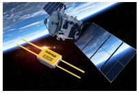
Renesas Electronics’
ISL70591SEH and ISL70592SEH
rad hard current sources. |
Rad Hard Current Sources For Sensing Subystems In Satellites
Photo: Offered in 4-lead ceramic flatpack packages or in die form, these rad hard, precision 100-µA and 1-mA current sources are said to offer a smaller footprint than competing current source ICs and discrete current source solutions. Targeting sensing subsystems in satellites, these current sources are well suited for telemetry, tracking and command, attitude and orbital control, and electrical power subsystem applications.
See the full story…
|
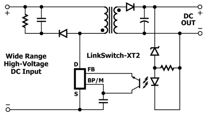
Power Integrations’
LinkSwitch-XT2
offline switcher ICs.
|
Flyback Switcher ICs Bring High Efficiency To Three-Phase 480-V Industrial Applications
Diagram: These offline switcher ICs, which incorporate 900-V power MOSFETs, simplify the design of high-efficiency isolated and non-isolated flyback power supplies up to 8 W, enabling a robust, low-component-count solution. These ICs are suitable for three-phase industrial power supplies to 480 Vac and consumer products destined for regions with unstable mains grids, tropical regions with frequent lightning strikes or areas where high-energy ring-waves and surges are prevalent..
See the full story…
|
|


|
|
MORE POWER PRODUCTS:
• Superjunction MOSFET Offers 900-V Breakdown Voltage And Low Total Gate Charge More details…
• Arbitrary/Function Generator Enables Engineers To Generate Test Signals Easily More details…
• LDO’s Miserly Iq Prolongs Battery Life While 1-mm2 Footprint Saves Space
More details…
|
|
 |
INDUSTRY EVENTS |
|
Symposium Tackled EOS And ESD Challenges Across The Electronics Spectrum Including Power Design
by David G. Morrison, Editor, HOW2POWER.COM
The recent EOS/ESD Symposium and Exhibits, held September 20-28 in Reno, NV, drew a total of 572 attendees to participate in tutorials, exhibits, workshops, discussion groups, technical sessions, invited talks and hands-on sessions on EOS and ESD topics. The symposium, which celebrated its 40th anniversary this year, was a unique forum for engineers to address their ESD challenges by learning best practices and discovering the latest technology for ESD control, protection and design. Moreover, it addressed EOS and ESD issues at the device, board and system level, making it relevant to engineers across the electronics spectrum, including developers of power semiconductors, power converters and power systems. Read the full story…
|
|
 |
WHAT'S NEW AT HOW2POWER.COM
|
Advice To Power Supply Designers (Part 2): The High-Performance Semiconductor Vendor Brings Value
 by P.S. Wacher, Semiconductor Industry Veteran by P.S. Wacher, Semiconductor Industry Veteran
In part 1 of this article for FAE Confidential, the author discussed how engineers working at power supply companies can identify the “needy” component vendors, who tend to waste the engineer’s time. Now in part 2, he explains how to identify those vendors who do bring value and help the customers design and build better products. Read FAE Confidential on our Home Page…
|
IN MEMORIAM… |
|
Milan M. Jovanović passed away on October 9. Dr. Jovanović was highly admired and respected for his contributions to the power electronics field, and as a mentor, colleague and friend to many. For more about his life and tributes from those who worked with him, see the Life Tributes page.
|
OTHER TOP POWER NEWS
|
|
Looking ahead to ECCE 2019 in Baltimore, the IEEE Energy Conversion Congress & Expo has issued its call for papers, call for tutorials, and call for special sessions. Paper digests are due January 15, tutorial proposals are due February 17, and special session proposals are due March 31. For more about this conference, see How2Power’s ECCE section.
On February 12-14, 2019, PowerAmerica will host its annual meeting on the campus of N.C. State. This meeting brings together leaders in the field of SiC and GaN power electronics.
CURENT, the Center for Ultra-Wide-Area Resilient Electric Energy Transmission Networks, has announced a DOE Traineeship Program for hands-on experiences with wide bandgap power electronics. This program offers fellowships for M.S. or Ph.D students. For more details, see https://potenntial.eecs.utk.edu.
Power supply manufacturer COSEL has announced a new R&D innovation center in Toyama, Japan.
Vitrek, a provider of high-voltage test and measurement equipment, has acquired XiTRON Technologies, a recognized source of precision power test and measurement solutions.
|
|
 |
|